admeta advanced
metallization
conference

KEYNOTE &
INVITED SPEAKERS

Keynote

session 2

Advanced Interconnect

The 3D Evolution in Transistor Architectures and its Impact on Advanced Metallization

Hans Mertens

                   
Affiliation
Principal Member of Technical Staff at imec
Biography
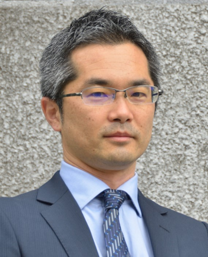
Hans Mertens is a principal member of technical staff at imec. He received a M.S. Degree in applied physics from Eindhoven University of Technology (2002) and a PhD degree in physics from Utrecht University (2007), both in The Netherlands. Prior to joining imec, he worked at NXP Semiconductors as Senior Scientist in the field of SiGe heterojunction bipolar transistors for RF applications.
His current research interests include novel integration solutions for advanced CMOS transistor architectures, including nanosheet FETs, forksheet FETs, and CFETs. He has published over 40 papers at the IEEE Symposia on VLSI Technology (VLSI) and at International Electron Devices Meetings (IEDM), of which 8 papers as a first author.

Invited Talks

session 3

Advanced Dry and Wet Processes

Depth-Controllable Passivation for Isotropic Etching and Advanced Profile Engineering

Tsubasa Imamura

                   
Affiliation
Senior Researcher at the Research & Development Group, Hitachi, Ltd.
Biography
Tsubasa Imamura is a Senior Researcher at the Research & Development Group, Hitachi, Ltd., where he leads the development of electron microscopes.He received a Ph.D. in Electronic Engineering from Nagoya University in 2021.
Prior to joining Hitachi, he worked at Toshiba, Toshiba Memory Corporation, and Kioxia Corporation, accumulating a total of 14 years of industry experience, including approximately 10 years in dry etching process development for 3D NAND devices.His research interests include semiconductor manufacturing processes, as well as gas etching and plasma etching processes.He has published four peer-reviewed journal articles and holds seven patents.

session 4

Advanced Packaging I

Surface and interface design for reversible interconnection

Akitsu Shigetou

                   
Affiliation
Principal Researcher at the National Institute for Materials Science (NIMS)
Biography
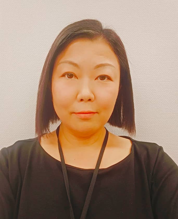
Dr. Akitsu Shigetou is a Principal Researcher at the National Institute for Materials Science (NIMS). She received her B.E., M.E., and Ph.D. in Precision Engineering from the University of Tokyo.
Her research focuses on the design and creation of functional surfaces and interfaces to achieve precise control over bonding and debonding properties. While this expertise is applied to semiconductor integration and packaging, her work primarily addresses the underlying surface science governing material integration. She also serves as a Visiting Professor at the University of Tokyo, bridging fundamental interface engineering with industrial applications.

session5

Atomic Layer Process (Joint Session with the JSAP Atomic Layer Process Research Group)

Towards Intelligent and Sustainable ALD Research: On-Demand Precursor Delivery and In-Situ Imaging Ellipsometry for Accelerated Process Development

Takeshi Momose

                   
Affiliation
Kumamoto University
Biography
Takeshi Momose is a Professor at the Research and Education Institute for Semiconductors and Informatics, Kumamoto University. He received his Ph.D. in Engineering from the University of Tokyo in 2009. After serving as an Assistant Professor and Lecturer at the University of Tokyo and an Associate Professor at Kumamoto University, he assumed his current position in 2024. He also serves as Special Assistant to the President at Kumamoto University, Program Director, Kumamoto University Semiconductor Reskilling Center, and Visiting Professor at National Chung Hsing University, Taiwan.

His research focuses on semiconductor thin-film deposition processes—including atomic layer deposition (ALD) and supercritical fluid deposition (SCFD)—and reaction engineering applied to advanced Cu interconnects, 3D packaging, and process informatics.

Atomic Hydrogen for Oxygen-Free Metal ALD and Bottom-Up Interconnect Fill

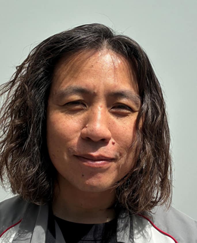
Han-Bo-Ram Lee

                   
Affiliation
Graduate School of Semiconductor Materials & Devices Engineering, Ulsan National Institute of Science and Technology (UNIST)
Biography
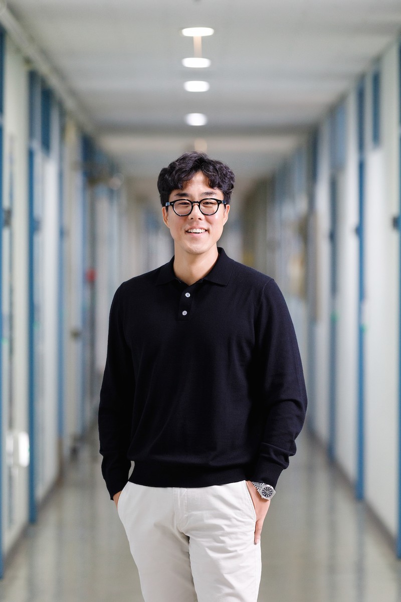
Han-Bo-Ram Lee is a Professor in the Graduate School of Semiconductor Materials and Devices Engineering at the Ulsan National Institute of Science and Technology (UNIST), Korea. He received his B.S. in Materials Science and Engineering from Sungkyunkwan University (2005) and his Ph.D. from POSTECH (2009), and completed postdoctoral training at Stanford University, where he later served as a visiting professor in Chemical Engineering.

His group, the HBRL Research Group, studies atomic-scale processing for semiconductor manufacturing — atomic layer deposition (ALD), area-selective deposition, and atomic layer modulation (ALM), a sub-monolayer composition-control technique his group pioneered — with a distinctive emphasis on bridging experiment and computation. By combining DFT, Monte Carlo simulation, machine-learned force fields, and generative AI, his team is building a digital twin of the ALD process environment, applied to high-k dielectrics and low-resistivity metals for next-generation devices. He has published more than 150 peer-reviewed papers, serves as Executive Editor of Chemistry of Materials (ACS Publications), chaired the International Conference on ALD/ALE 2025, and serves on the ALD/ALE Steering and AVS Program Committees. He is also a consulting professor with SK hynix.

session 6

Materials Science and Technology

Metallic delafossites for low-resistivity advanced interconnects

Takayuki Harada

                   
Affiliation
Principal Researcher, National Institute for Materials Science (NIMS), Japan
Biography
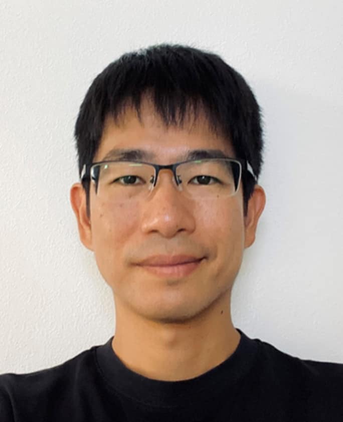
Takayuki Harada is a principal researcher at the National Institute for Materials Science (NIMS), Japan. He received a Ph.D. degree in applied chemistry from the University of Tokyo (2011). Prior to joining NIMS, he worked at Institute for Solid State Physics in UTokyo, Max Planck Institute for Solid State Research, and Institute for Materials Research in Tohoku University.
He is focusing on exploratory research on thin-film heterostructures.
He has published about 40 peer-reviewed papers and holds 2 patents. Recent honors include the MEXT Prize for Young Scientists.

session 7

Advanced Packaging Ⅱ

Development of a test platform to evaluate process variables for copper hybrid bonding technology

Kyung-Ho Park

                   
Affiliation
Principal Researcher
Korea Advanced Nano Fab Center (KANC), Korea
Biography
Kyung-Ho Park is a principal researcher at Korea Advanced Nano Fab Center (KANC), where he leads the advanced packaging TF.
He received a Ph. D. in applied physics from Ajou University in Korea (2002).
Prior to joining the advanced packaging TF, he worked at the convergence technology division as a general manager (vice president).
His research interests include semiconductor advanced packaging technologies such as Cu hybrid bonding, silicon bridge, and RDL (Redistribution Layer).
He has published 81 peer-reviewed articles and holds 43 patents. Recent honors include a commendation from the Minister of Science and ICT of the Republic of Korea.

Challenges for half micron pitch damascene pattern fabrication for organic RDL in next generation’s Chiplet technology

☆ Yoshihiko Hirai

                   
Affiliation
Professor of Physics and Electronics Engineering, Graduate School of Engineering, Osaka Metropolitan University
Biography
Y. Hirai, 1980-1997 Matsushita Electric Industrial Co., 1997-2020 Osaka Prefecture University, 2020 Osaka Metropolitan University, Appointed Professor of Osaka Metropolitan University

Masaru Sasago

                   
Affiliation
Professor of Physics and Electronics Engineering, Graduate School of Engineering, Osaka Metropolitan University
Biography
M. Sasago, 1978-2021 Matsushita Electric Industrial Co., 2021 Osaka Metropolitan University,  Appointed Professor of Osaka Metropolitan University

Shinji Kishimura

                   
Affiliation
Visiting Professor of Physics and Electronics Engineering, Graduate School of Engineering, Osaka Metropolitan University
Biography
K. Kishimura, 1986-1998 Mistubishi Electric, 1999-2014 Panasonic Corp., 2014-2016 University of Tokyo, 2016-2025 Kyoto University, 2025 Osaka Metropolitan University, Visiting Professor of Osaka Metropolitan University